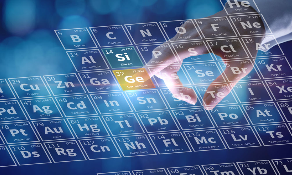
GeSi
The next frontier of photonic technology for sensing and
connectivity
Germanium (Ge) had a long history in the semiconductor industry. At the electronics side, two physicists at Bell Laboratories in the US — John Bardeen and Walter Brattain — demonstrated the first solid-state transistor by using two thin gold contacts into a slab of germanium in 1947, where their work was later awarded with Nobel prize in 1956.
Although Ge played a leading role in the early history in semiconductor, due to factors such as that its material surfaces are harder to passivate and Ge wafers are more difficult to grow in large diameters compared to silicon (Si), Si-based technology such as CMOS (complementary metal-oxide-semiconductor) transistor eventually dominated and became a commercial success. Since then, Ge was predominately used in SiGe, an alloy containing a small portion of Ge in Si matrix, for specialized applications such as SiGe HBT (heterojunction bipolar transistor) in BiCMOS (bipolar CMOS) transistors, or source and drain strain engineering in CMOS transistors.
While Si has many advantages, it is noteworthy that at the photonics side, Si does not interact with light efficiently, especially at the SWIR spectrum. While there have been attempts on making PDs (photodetectors) with plasmon-induced hot electron injected from metal to Si, these devices still suffer from low QE (quantum efficiency), high dark current, and slow operation speed. Therefore, group III-V compounds became the next matured semiconductor material platform following Si for specific RF (radio-frequency) microelectronics and optoelectronic applications. However, III-V materials are more expensive than Si, and are difficult to integrate with mainstream silicon-based technology.
To overcome these decades-old challenges, Artilux has been dedicated on fundamental physics to not only achieve quantum leap performance enhancement, but also make this technology ready for commercialization.
Silicon (Si) and other basic functional materials

Predominately represented by Gallium Arsenide (GaAs), Indium Phosphide (InP) as well as certain group III-V compounds

Silicon Carbide (SiC), Gallium Nitride (GaN) etc. high bandgap materials

After years of dedication and relentless innovations, Artilux has achieved the unachievable and brought Ge back to the spotlight, unveiling a new generation of germanium-silicon (GeSi) technology. By overcoming several critical technical challenges ranging from heterogenous material engineering, nano-scale electrical field and optical field control, and wafer-level electronics/photonics integrated designs, Artilux has successfully launched this technology on CMOS production line through close collaboration with TSMC, and has been recognized as the worldwide leader of wide spectrum, i.e., NIR (near infrared)+SWIR (short-wavelength infrared) sensing and 3D sensing technology, both are ready for commercialization at scale.
The capability to detect both NIR and SWIR wavelengths on mature CMOS technology platform has opened up exciting opportunities in applications such as LiDAR (light detection and ranging), 3D sensing, proximity detection, AR (augmented reality) and VR (virtual reality), to name a few.
Artilux’s GeSi technology solves existing physics and engineering bottlenecks by significantly increasing QE across a wide spectrum from 940nm all the way to 1550nm and beyond. Combined with low dark current characteristics that unlock operations from low to ultra-high modulation frequencies, Artilux’s GeSi technology delivers higher accuracy and better performance in sunlight and greatly reduces the risk of eye damage — all at a competitive price and ready for mass production.

Tailoring to fundamentally different operating principles and requirements for different target applications, Artilux has developed a comprehensive GeSi technology family that includes:
Artilux’s continuing breakthroughs will not only benefit the optical sensing and imaging industry by enabling the most advanced GeSi technology on cost-effective CMOS technology platform, but will also re-define the role of Ge in the semiconductor history.